Last Updated on October 29, 2019 by nghiaho12
This is a follow up on my previous post about my first step into the FPGA world. In this post I’ll give a high level description of my implementation of a simple 3×3 convolution image filtering circuit. It does not aim to be fast or efficient, just something that works. If you want to know anything in more detail look at the code or leave a comment below.
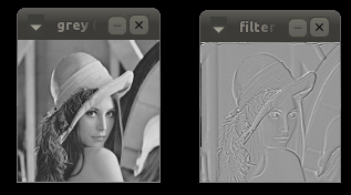
I’ll assume the reader is familiar with 3×3 filters like the Sobel edge detector. In this project l implement the Laplacian filter, but you can easily change the filter by changing the hard coded values inside the Verilog file.
Below is a high level overview of my FPGA design. I’ve omitted the input/output pins for each of the block component for simplicity.
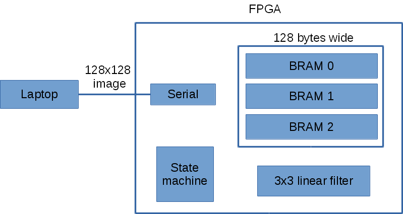
The laptop sends the image over the serial one row at a time to the FPGA. The FPGA then immediately sends the processed pixel row back to the laptop. I chose this design because it only requires three row buffers on the FPGA. The Basys2 has 72Kbits of fast RAM. For an image width of 128 pixels, it only requires 128×3 = 384 bytes of RAM.
The state machine handles all the logic between the serial, BRAM and 3×3 linear filter.
I decided to use serial for communication between the laptop and FPGA because it was simpler, though slower. I did however manage to crank up the serial speed to 1.5 Mbit by adding an external 100Mhz crystal oscillator. Using the default 50Mhz oscillator on the Basys2 I can get up to 1 Mbit.
I use three banks of dual port BRAM (block RAM). The dual port configuration allows two simultaneously read/write to the same BRAM. This allows me to read 3×2=6 pixels in one clock cycle. For 3×3=9 pixels it takes two clock cycles. I could do better by making the read operation return more pixels. The three banks of BRAM act as a circular buffer. There’s some logic in the state machine that keeps track of which bank of BRAM to use for a given input pixel row.
Right now with the my current BRAM configuration and 3×3 filter implementation it takes 5 clock cycles to process a single pixel, excluding serial reading/writing. If you include the serial transmission overhead then it takes about 380 ms on my laptop to process a 128×128 grey image.
Below is the result of the Laplacian filter on Lena. I ignored the pixels on the border of the image, so the final image is 126×126.
Download
The zip file contains only the necessary Verilog code and a main.cpp for sending the image. The main.cpp requires OpenCV for display. I omitted any Xilinx ISE specific project files to keep it simple. But if there’s any missing files let me know. Your input image must be 128×128 in size to work.